 | ||||
 | ||||
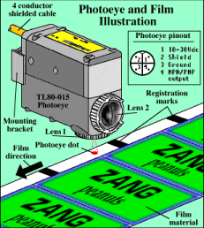
20 Bit Asynchronous 5 Digit Counter with Displayed Memory of the BFC 9000 After working at Starbucks Coffee for a couple of years, I have gained experience in the manufacturing process of consumer goods packaging. At the Starbucks roasting plant, for instance, they roast the coffee and it needs to be put into small packages of various sizes depending on the consumer market being targeted. As with Starbucks, almost all consumer goods (including non-food items) have some form of packaging lines to protect their products and keep them fresh for sale. And to package these products, certain materials are needed to make this happen. The most popular is some form is a sheet like material that can be shaped and sealed to hold in freshness and keep foreign substances out (like a sealed bag of coffee) that is termed Packaging Film. These materials are purchased by the manufacturer on huge rolls and are fed into automated machinery to that large production runs can be accomplished with a minimal of cost. Most of this Film needs to be cut at exact intervals as they pass through the machinery so that any product titles and/or graphics are the same for each individual product. This is done with the aide of printed markings on the Film so the machine knows where to seal and cut the Film. These marks are called Photo Registration Marks. These marks trigger a photoeye that makes the machine cut the impression at the appropriate position on the bag (Photoeye and Film Illustration.) By connecting to that pulse to a digital counter, a tally of every film impression is made so that inventory control can keep track of how many impressions of that Film was used, and not used, for actual finished goods. It is normal for a certain amount of Film (or other related materials) to be wasted in setting up machinery and for other problems encountered, for a production run. Also, it is common-place for goods to be produced but they cannot be released to consumers for a number of packaging defect reasons. The initial keeping track of materials used in a production run is done by a Machine Operator. With the aide of this counter, the Operator can easily see what Film is used for good product and what was thrown away. At certain intervals, this Operator can find their scrap total by reading the saved number on the display. Then subtract the total good product released to inventory from that number. The difference was lost somewhere in scrap materials used during their shift. This can be recorded where applicable for inventory control purposes and keep track of production costs. Below is a detailed description of how the circuit works and the design of each sub-circuit. Please scroll through the list, or click on a bulleted circuit description in the Detailed Operation Target List to jump to that circuit. At the end of each description is a link back to the Target List. Each graphic thumbnail is clickable for a larger view. Detailed Operation Target List
Circuit Overview
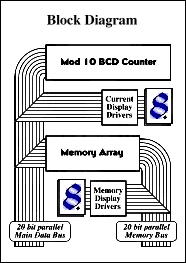
This device consists of 8 sub circuits. It starts with a digital counter, data bus and a display that shows the value of the counter. There is a memory array that reads the dada bus and displays what the previous value of that bus was prior to the pressing of the Save/Reset button. The block diagram here illustrates the basic circuit design. The circuit uses a variety of TTL 74nnn series IC's. Some of the circuitry today can be simplified by used dedicated IC's (like the Mod 10 counter for instance, a single LS74143 (4 bit counter/latch, 7 segment LED/lamp driver) could have been used to replace many circuits here but for the purpose of education, we opted for the long route. A complete parts list is as follows. Refer to an updated TTL book for specific specs on each component. There's too much to list here. IC's
Components
Misc. Parts
Detailed Operation of Mod 10 Counter
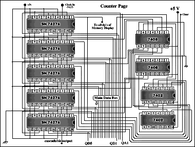
The counter starts with an input signal from an electronic photoeye circuit to the first of five cascaded LS74276 quad J-K flip flops (the photoeye circuit is described in detail later.) Each flip flop is setup as a Mod 10 counter with the use of LS7408 NAND gates. The output signal from these flip flops make up a twenty bit data bus. We could have opted to use dedicated Mod 10 IC's (LS74143) but for the purpose of education we went the long route. This circuit is a asynchronous (ripple) counter. Each J K flip flop depends on the output of the previous J -K flip flop. When each respective input goes to the high state (a binary 1) it triggers the output Q to change state. This creates a binary frequency divider that cascades to each flip flop. The flip flops are arranged with the Least Significant Bit (LSB) on the right. The LSB's are on the right so that the order of the flip flops are the same as the order of the bits in the binary count. The numbering system for all 5 flip flops start at A0 up to A19 giving the 20 bit data bus. Each FF has a asynchronous CLEAR input, these are connected together to the output of a two-input NAND gate with inputs J-K 1 and J-K 3. When each of the 4 J-K flip flops in each successive IC reach 1010, the NAND gate resets the chip to 0000 and the Next Significant Bit on the next set of 4 flip flops in the next IC will trigger one. The final configuration makes one 20 bit cascaded binary frequency divider where each bit is changed by the positive going transition of the previous IC's final output. Visual Interface
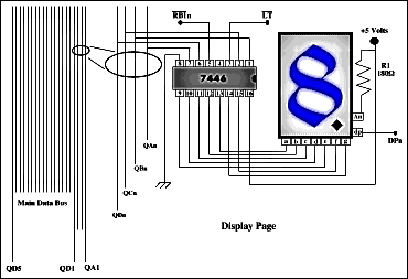
Five 7 segment/decoder drivers read the data bus and display the numerical equivalent on the 7 segment display. This numeral display can display a decimal value up to the 10-Thousands place. This number can be reset to zero by pressing the reset button (described later.) It is possible to add additional flip flops and displays if higher values are desired. Another 5 drivers and displays were used for the memory circuit described next. Note: The seven segment display decoder/drivers come in 2 versions. The LS7446, Ô47, Ô49 are common Anode displays. The LS7448 uses a common Cathode display. We opted to use the LS7446. The LS7448 is harder to find and it utilizes an internal 1k* pull-up resistor making the display relatively dim. Not only that, the '48 is more expensive, about $5+ each as opposed to about $2.50ea for the others. Each output of the LS7446 should contain a current limiting resistor with a value of about 250*. For this circuit, one limiting resistor was used on the ground side. This caused the individual segments to show at different brightness' depending on just how many of them were illuminated. The more segments that were lit, the dimmer the display became. Memory System
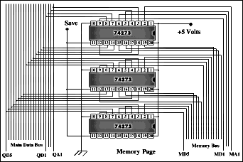
In the circuit there are three LS74273 chips (Quad D FF register.) This chips are connected to the data bus and when activated by a high state on the latch input it reads the information on the data bus. When the latch goes low, the IC's don't read the contents of the data bus when it changes it's binary value. This data is stored only when the Store/Reset button is pressed and released (again described later.) The memory IC's then output the stored binary value to another 20 bit data bus where another 5 display/decoder driver IC's display the stored value. Blanking Zero Circuit
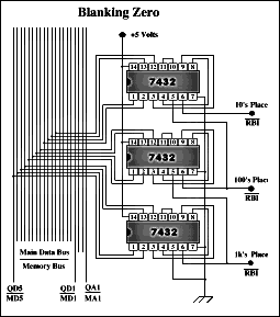
The blanking zero circuit was added for aesthetics. By reading the Main Data Bus for the MSD with LS7432 OR gates, the Higher Significant Digit on the displays would show an actual whole number. Without this, the number __605 would not read as __6_5 (where a _ is an unilluminated 7 segment display.) When any of the outputs to the RBI (Ripple Blanking Input) of the decoder driver IC's from the LS7432's were low, then that display would show an actual "0" if there was a value of 1 or higher in the next significant digit. Memory Storing Circuit
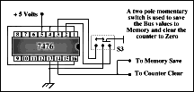
By using an LS7476 dual J-K flip flop IC, we could provide the High and Low stated required to cause the memory circuit to store the contents of the data bus in memory and reset the counter circuit to 00000. With a single push of a momentary pushbutton oe of the two flip flops are triggered. When the button is depressed, the input went low to the flip flop. When the button is released, a low pulse was created causing both the counter clear and the memory latch to activate. During initial construction a problem presented itself. The time taken by the memory IC's to read the Main Data Bus while the counter was resetting was too short. This results in a no-save (or a save of Ò00000Ó). Both the counter clear and the memory latch needed to go low, but enough delay between the two. What was needed was propagation delay. This was inadvertently created by the 7402 NOR gates on the Counter Page which were modified slightly to accommodate this in the final design illustrated here. Photoeye Circuit
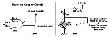
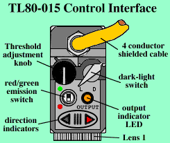
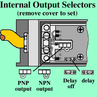
The most critical implementation of the circuit was the photoeye circuit. Although very basic in design, is was necessary to couple the output from an industrial grade photo registration mark reader to a triggered 5V output. This was accomplished by taking the output from pin 4 from the photoeye assay below (refer to the Photoeye image.) This output pulse triggers an NPN 3904 transistor in a +5V pull-up configuration. An additional LED was placed between Rc and the transistor for an added visual indication that the proper trigger was taking place from the circuit. A manual trigger pulse momentary switch was added for testing purposes. The power to the photoeye was set at about 12V dc. The Photoeye Control Interface allows the user to select what conditions will trigger the photoeye. This is dependent on the colour of the Registration mark and the background colour of the film. There are specific instructions per each photoeye depending what type of brand you get. Refer to your own data sheet for details. With this model you could remove the cover and select what type of out is send out (NPN/PNP) and wether there's an internal delay or not. | ||
 |  | |||||
 | ||||||
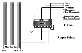
Rippling Decimal Point
This sub-circuit was added to give a quick visual representation that a trigger was happening. This was accomplished by installing a LS7442 4-line BCD to 10-line Decimal Decoder to decode the first four bits on the Data Bus. Every other output from this decoder was ran to the Data Bus's display decimal points. This resulted in visual directional "movement" of the respective decimal points. If desired, all 10 outputs could go to ALL decimal points on both the current counting display and the saved number on the other 5 7-segment displays. Display Proveout Test
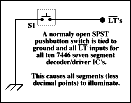
This was a simple diagnostic tool that was added last. A built in function of the 7-segment decoder/drivers is a Light All Segments function. When Pin 3 LTnot goes LOW then all segments illuminate. If there was a question if an LED was burned out or another problem existed, pressing the button as illustrated could show the technician if the display circuits worked correctly. If a segment or two didn't illuminate, then either there's a concern with the driver chip, the LED displays or the wiring in between Circuit Prototype Photo
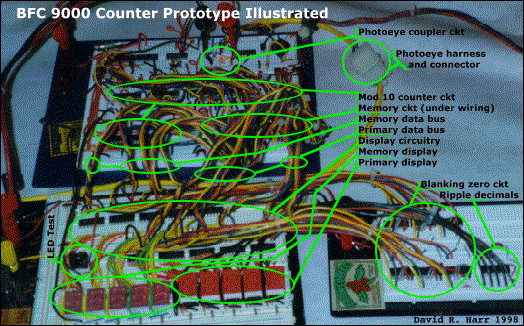
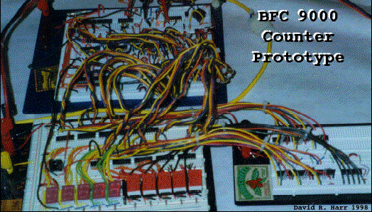
| ||